


- Synthesis, Structural, Time-Dependent Density-Functional Theory, Thermal Annealing and Optical Properties for Doped Polymer Nanostructured Thin Films as Optoelectronic Devices
Ahmed F. Al-Hossainy†
 and Mohamed Sh. Zoromba*, **
Department of Chemistry, Faculty of Science, Northern Border University, 13211 Arar, Saudi Arabia
*Chemical and Materials Engineering Department, King Abdulaziz University, Rabigh 21911, Saudi Arabia
**Department of Chemistry, Faculty of Science, 23 December Street, 42521, Port-Said University, Port-Said, Egypt- 광전자소자로 이용가능한 나노구조 poly(4-phenylenediamine-co-2-aminophenol) 박막의 제조 및 분석
Reproduction, stored in a retrieval system, or transmitted in any form of any part of this publication is permitted only by written permission from the Polymer Society of Korea.
The dependence of structural and optical characteristics on the thermal annealing of a doped poly(4-phenylenediamine-co-2-aminophenol) nanostructured thin film [P4D2AP]TF as a doped polymer conductor nanostructured thin film was studied. [P4D2AP]TF was fabricated as a thin film (100 ± 2 nm) using the spin coating method. Various characterization methods for [P4A2AP]TF like Fourier-transform infrared spectroscopy (FTIR), ultraviolet-visible spectroscopic (UV-Vis), thermogravimetric analysis (TGA), and optical characteristics have been studied. The resulted X-ray diffraction (XRD) and scanning electron microscope (SEM) data have been employed to study interface composites. Density functional theory (DFT) was used for optimization by atomic orbital DFT code (DMol3) and Cambridge serial total energy package (CASTEP). Spectroscopic and structural characteristics for the thin film have confirmed the chemical composition and XRD observations revealed the same crystal structure. The fabricated film was annealed in the air for 1h at 100 and 200 oC. XRD examination of [P4D2AP]TF displayed that symmetry is an orthorhombic with a space group (Pmcn). The optical characteristics demonstrated that the thin film has a relatively high absorbance of 95%. The calculated energy gaps are 2.523 eV and 2.504 eV for DFT and experimental, respectively. In addition, the optoelectrical parameters of the film have been calculated for absorption index (k(λ)), refractive index (n(λ)), dielectric constant, and optical conductivity. CASTEP simulated values are consistent with the experimental values for optical parameters of [P4A2AP]TF. The findings of the structural and optical characteristics described the fabricated thin film can be utilized as a candidate material for optoelectronic devices and solar cells.
The dependence of structural and optical characteristics on the thermal annealing of [P4D2AP]TF as a doped polymer conductor nanostructured thin film was studied. [P4D2AP]TF was fabricated as a thin film with  100 ± 2 nm using the spin coating method. The findings of the structural and optical characteristics described the fabricated thin film can be utilized as a candidate material for optoelectronic devices and solar cells.
Keywords: synthesized poly(4-phenylenediamine-co-2-aminophenol) nanostructured thin film, X-ray diffraction, scanning electron microscope, time-dependent density-functional theory, thermal annealing, optical characteristics.
The authors gratefully acknowledge the approval and the support of this research study by the Project no SCI-2019-1-10-F-1112 from the deanship of scientific research at Northern Border University.
Information is available regarding the experimental section (materials and reagents, synthesis of doped P4A2AP copolymer, fabrication of the [P4A2AP]TF, and computational study) and results and discussion section (Combined experimental and simulated XRD, Geometry computations ED, P and MEP for P4A2AP isolated molecule). The materials are available via the Internet at http://journal.polymer-korea.or.kr.
PK_2021_045_04_541_Supporting_Information_template.pdf (481 kb)
Supplementary Information
Conjugated polymers have been interested in many researchers because of their different applications, and their great properties including inordinate stability in the open air, corrosion resistance, and flexibility.1,2 Aniline derivatives have been displayed a specific reflection because of their fascinating conductivity and great optoelectrical properties. Polyaniline derivatives have several applications such as molecular electronic devices,3 batteries,4 electrochromic apparatus,5 photoelectrochemical cell.6 To improve the conductivity and solubility of polyaniline, copolymer of polyaniline derivatives has been carried out. Moreover, nanostructured thin films of the resulting polymers were synthesized by using different routes including traditional surface interfacial polymerization, electrodeposition, spin-coating, or thermal-evaporation route.7 In addition, thin films have been fabricated from conducting polymers have several potential manufacturing implementations like solar cell applications.8 Poly(o-phenylenediamine) (PoPD) is a semi-conductive homopolymer that can be used to manufacture ortho phenylenediamine monomers in the acidic aqueous medium by means of electrochemical or chemical polymerisation.9 PoPD has different applications including electrochromic devices and sensors, microelectronics, electrocatalysts.10 The thin film of PoPD is suitable for several applications including pH-sensors, corrosion resistance, electron transport mediator, electrochemical diode, and perm selectivity. On the other hand, ortho aminophenol monomer is one of the aniline derivatives that have the feature to give numerous coordination sites because of the presence of (-NH2) and (-OH) groups connected directly to the benzene ring.11 Moreover, the electrochemical process for poly(o-aminophenol) synthesis requires the formation of phenoxazine devices to fabricate new conducting materials o-aminophenol permits the creation of o-aminophenocazine through chemical oxidation polymerization methods.12,13 The copolymerization of aniline o-aminophenol was performed to enhance the solubility and electric conductivity of poly(o-aminophenol). In particular, copolymer synthesis has been greatly influenced by polymerization conditions including a concentration ratio of monomers, acid levels, and possible applications.14,15 Several neat polyaniline derivatives or copolymers of polyaniline derivatives have been reported.16,17 Thermal annealing plays a major role in change morphology for amorphous conductor polymers specially, in the relationship among glass transition temperature (Tg) and melting temperature for the polymer.18 For example, if the melting point temperature of polymer thin films is smaller than Tg, the fabricated polymer chains are chiefly immobile, thus maintaining the present morphology. On the other hand, if the annealing temperature is larger than Tg, the fabricated conductor polymer thin film matrices will be stable and fix.19 It has been found that the morphology can be changed upon annealing at a temperature larger than Tg, consequently, change the physical properties of the fabricated conductor polymer thin films will be carried out.20
The present work aim was planned not just to modify the synthesis and structure of [P4A2AP]TF for potential incorporation in optical diode but also for satisfactory the demanding essential for vision into the applicable physical methods that characterized the charge transfer in these films. This emphasizes the importance of controlling deficiency states in polymer molecular crystals in order to achieve the favored photoelectric properties. Besides, A full density function theory (DFT) study of HCl-doped poly(4-phenylenediamine-co-2-aminophenol) (P4A2AP) structures combined with Rietveld refinement technique is applied. The experimental calculations for a fabricated thin film of P4A2AP were compared with the theoretical one. In the case of doped P4A2AP matrix structure models, the synchrotron X-ray powder-diffraction (SXPD) pattern was used to compare their simulated diffraction formations. The optical properties are studied for the fabricated [P4A2AP]TF by spin coating technique at different annealing temperatures on quartz substrate. Finally, the comparison among the optical properties of the doped [P4A2AP]TF thin-films and Cambridge serial total energy package (CASTEP) computations is determined.
Characterization. Fourier Transform Infrared Spectroscopy (FTIR)/KBr pellets were measured by utilizing a Perkin-Elmer FTIR type 1650 spectrophotometer (United States) in 400 ≤ wave number ≤ 4000 cm-1. Thermogravimetric analysis (TGA) and DrTGA/N2 gas is measured by utilizing DTG-60H Shimadzu simultaneous DTA/TG apparatus (Japan) at a heating rate of 10 oC min-1. X-ray diffraction (XRD) of the films are measured by XRD (Philips X` Pert-Pro MRD/λ=1.5418, Netherlands) utilizing Cu Kα radiation. The surface structure is investigated by Inspect S, FEI, Holland/3.0 kV electron microscope (Thermo Fisher Scientific, United States) for the fabricated thin-film and annealed [P4A2AP]TF. The cleaning process has been carried out by using Scientz SB-4200DT 14.4L ultrasonic cleaner (China). The spin coating has been carried out by using SPIN150i spin coater (Germany). The film thickness for [P4A2AP]TF are determined by used M-2000 Ellipsometer (United States). Finally, the optical parameters were recorded at l = 300-1100 nm utilizing SHIMADZU UV-3101UV/vis-NIR pc spectrophotometer (Japan).
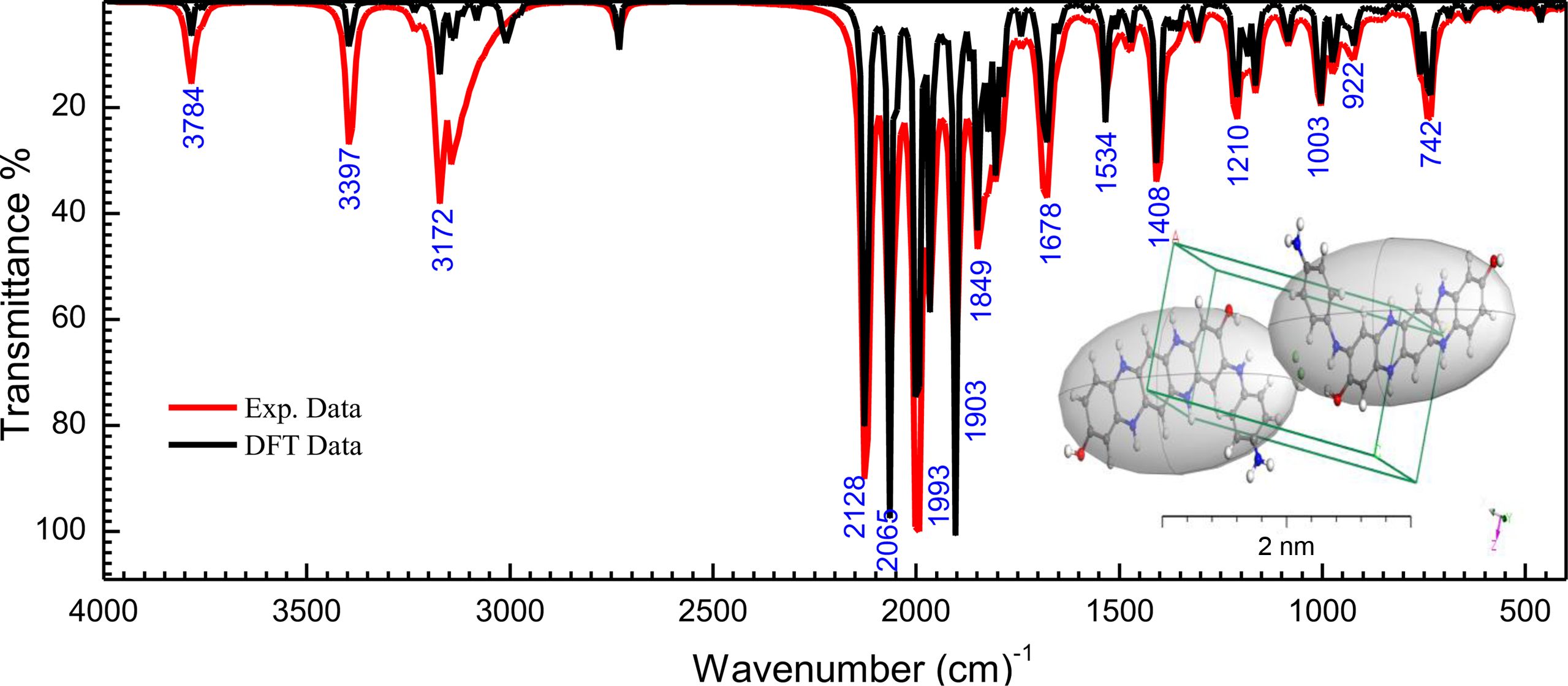
Fourier Transform Infrared Spectroscopy (FTIR). The stretching frequency (n) and bonding vibrations of functional groups for [P4A2AP]TF thin-film backbone are measured by FTIR spectroscopy. From Figure 1, the intermediate band at 3784 cm-1 is due to the stretching n(OH) in ortho-aminophenol (2-AP). The spectrum of [P4A2AP]TF illustrates a strong stretching band at 3397 cm-1 due to (-NH) group. The notation recommended by Wilson is utilized for the objective of the appointment. the [P4A2AP]TF, the bands noted within the range of 690-750, 830-950, 1350-1415, and 3050-3300 cm-1 are due to the wagging vibrations, rocking, bending, and stretching of OH group, correspondingly. This is attributed to the existence of H2O between the copolymer chains. At wavenumber around 2100-1600 cm−1, the absorption bands were detected, and this is attributed to stretching n(CH) of the aromatic ring.21-23 Moreover, FTIR spectroscopy reveals the characteristic bands of copolymer [P4A2AP]TF thin film. The [P4A2AP]TF thin-film spectrum demonstrated these absorptions due to the H-bonding aromatic groups of [P4A2AP]TF thin-film matrix. The stretching vibration for [P4A2AP]TF thin film at area 1600 cm-1 ≥ l ≥ 1350 cm−1, which attribute to n(CH). The strong band at 1210 cm-1 is a feature of [P4A2AP]TF thin film (doped with chloride ions on the nitrogen atoms of copolymer chains). The simulated IR computations for the P4A2AP gaseous phase matrix at 6-311G/DFT is demonstrated with Gaussian 09W/WBX97XD. The DFT-Gaussian 09W vibration values are very similar to the findings of the experiments. The theoretical IR spectrum was evaluated to give the spectroscopic signs of the P4A2AP isolated molecule gaseous phase. Comparison among experimental and simulated data is the small changes among the predicted and measured frequencies are shown in Figure 2. The key factor for the difference is that the count was measured in a vacuum whilst processing for a solid-state was calibrated.24,25 For P4A2AP gaseous phase of the isolated molecule, the following equation: λCal. = 0.0014lExp. + 12.41 with correlation coefficients (R2 = 0.999) described the direct-correlation between the computed (λCal.) and experimental wave-numbers (λExp.).
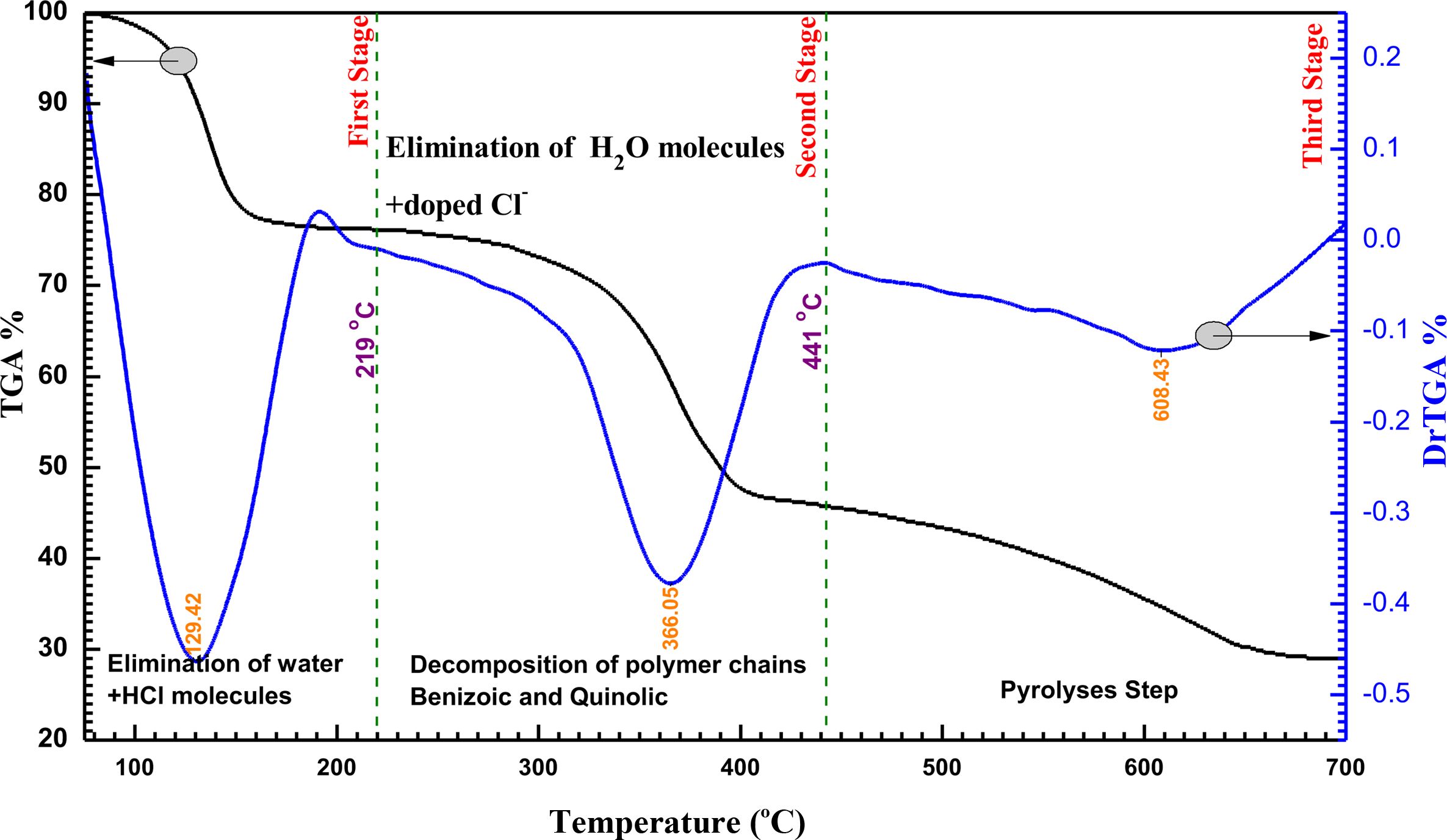
Thermal Analysis of P4A2AP Powder. The thermal stability of the copolymer has been studied at a heating rate of 10 °C/min in the inert atmosphere of nitrogen. Figure 2 displays the TGA and DrTGA curves of the copolymer powder. The curves show several peaks at 75-700 °C. From the thermogravimetric analysis, it can be observed that there are their different stages for the decomposition of the copolymer. The initial degradation stage carried out within the range of 75-219 °C with the exothermic step of TDrTGA at 129.42 °C (Tg), equal to the mass weight loss 24%.26 The loss of mass percentage in this stage can be attributed to removal (doped Cl- + H2Ocoordinate) from copolymer chains.27 The second degradation stage has been carried out within the range of 219-441 °C, the mass loss percentage is ≡ 30% which result from the decomposition of copolymer chains to oligomer which seems at the exothermic stage at 366.05 °C. The third degradation stage has been carried out within the range of 441-700 °C, the mass loss percentage is ≡ 17%. This is due to the carbonization of the polymer which appears at the exothermic step at 608.43 °C.
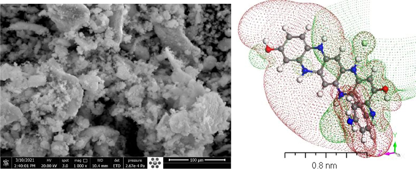
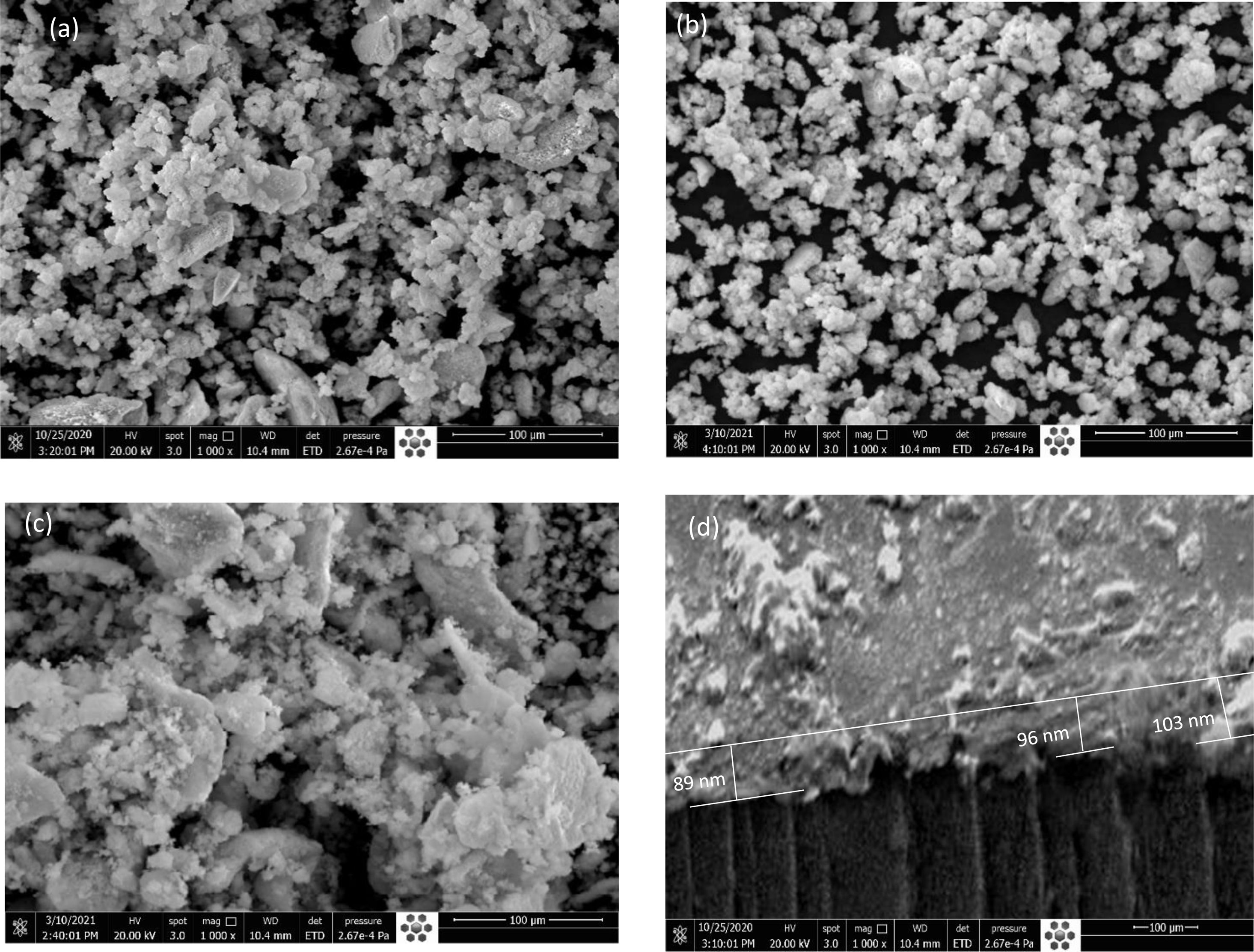
Surface Morphology and Crystalline Structure Charac- terizations. The surface microstructure of the [P4A2AP]TF thin film was investigated by scanning electron microscope (SEM). As illustrated in Figure 3(a-b) SEM images of the front and side [P4A2AP]TF thin film, both sample types displayed a dense and uniform surface microstructure. Although the [P4A2AP]TF thin film showed low crystallinity according to the SEM images. Since the sample displayed similar surface morphology and a distinct microstructure could not be observed in the SEM images, the highest crystallite-sized sample and grain size ≡ 50-70 nm were displayed in Figure 3(a). This result is in parallel with the XRD data of these films. While Figure 3(d) shows that the film is a homogeneity profile. The thickener of film calculated by the SEM process is @ 96 nm, with grain size estimated by SEM procedure is equivalent with the determined data by the M-2000 Ellipsometer. From SEM images (Figure 3(b) and 3(c)), it can be observed that the size of particles is bigger in Figure 3(c) (annealed at 200 °C) than the particle size in Figure 3(b) (annealed at 100 °C). The annealing may cause the agglomeration of particles. The average crystallite size (Dav) of [P4A2AP] TF increased with the thermal annealing increment which indicates the direction of large grain growth due to thermal annealing.
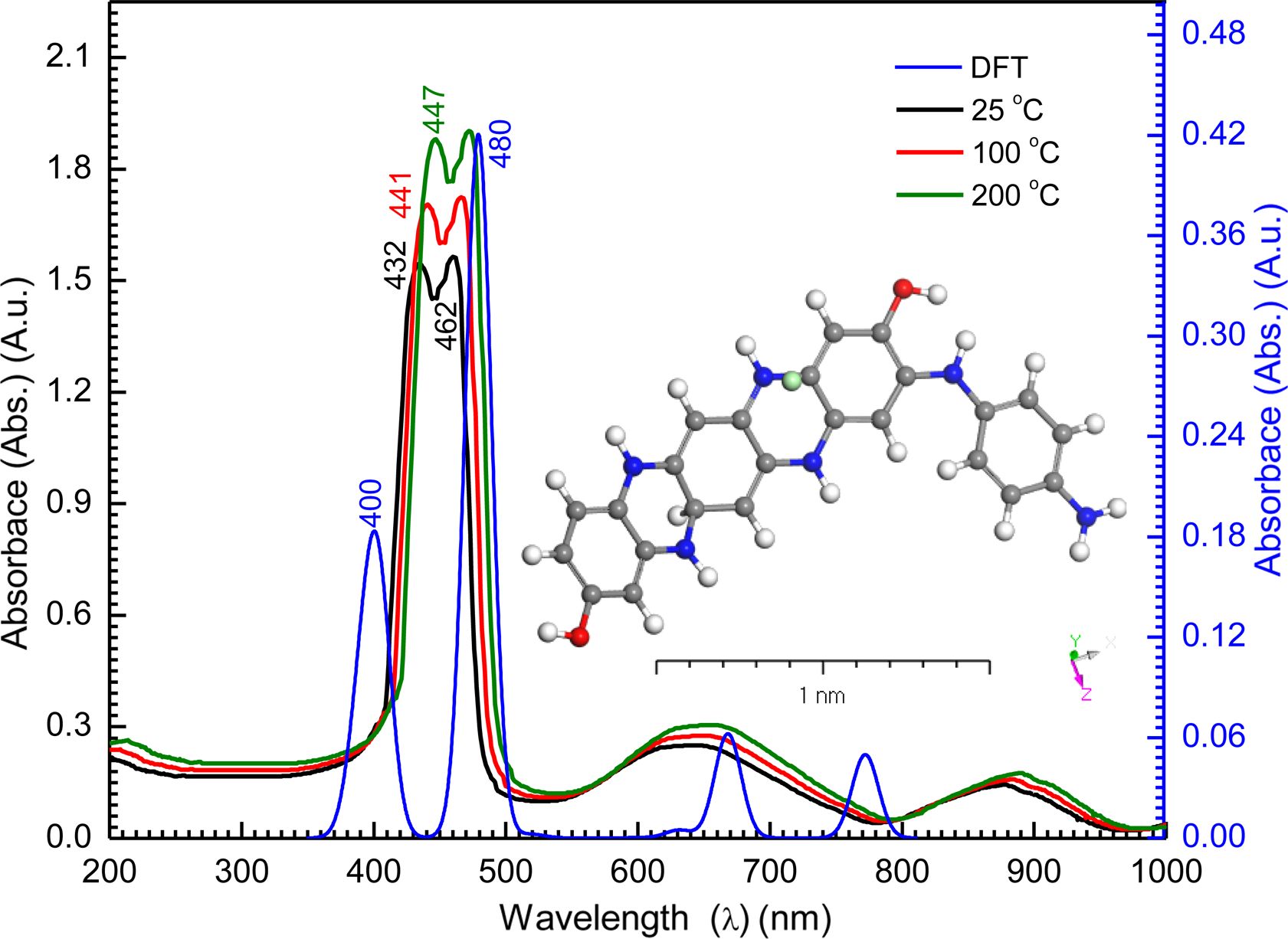
Optical Properties of [P4A2AP]TF. Transmission and Reflection Characterizations: The measurements of the UV-Vis absorption play a significant role in the determination of optical characteristics of any nanostructural semiconductors. The absorbency for [P4A2AP]TF in both UV-Vis and near-IR spectra areas was obtained at 25 °C, as shown in Figure 4. The [P4A2AP]TF shows extreme absorption called the Soret band, which showed up within the 375-475 nm wavelength range. Also, the Soret band appears with an intensity that is comparatively higher than that of the other bands in the pattern. Even the Soret band appears in the pattern with an amplitude that is comparatively higher than the other bands. In addition, it can be found that the characteristic splitting (Davydov splitting) is seen in this band.28,29 Application of model modified byKasha et al.,30 the sharp Soret band appears at Sx = 432 nm and Sy = 462 nm. Which is attributed to the splitting or shifting of the absorption band (Parallel electric dipoles).31,32
On the other hand, the band of the [P4A2AP]TF molecule, namely Q-band seems within the range of 525-1000 nm. This noticed Q-band contains multi weak peaks (i.e, six weak and broad bands). It is observed that the absorption peak intensity does not depend on annealing temperature, throughout the whole spectrum (200 nm ≤ λ ≤ 1000 nm). The peaks will usually be viewed as excitations among bonding and anti-bonding molecular orbital molecules in terms of π-π*.33,34 As the electric dipoles are oriented to the opposite end and electric dipoles cancelled, Q-band absorption transitions have diminished oscillator powers, contributing to the lower amplitude of the Q bands. From inset Figure 4 (simulated absorption using atomic orbital DFT code (DMOl3)/DFT method), a combination of experimentally and DMOl3/DFT calculations a good agreement of the maximum absorption with l(nm) and electronic transition of the [P4A2AP]TF copolymer.
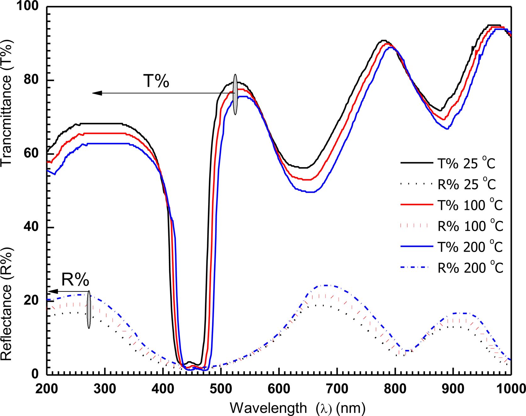
The fabricated film displays the highest optical-transmittance and reflectance. The performance of transmittance (T(λ))% and reflectance (R(λ))% for [P4A2AP]TF in the transparent-area are showed in Figure 5. Additionally, Figure 5 depicts that the spectrum can be separated into three different areas: (a): within the range of 300-375 nm, the full sum of the R(λ)% and, T(λ)% is approximately equal unity (transparency-region). (b): within the variety λ=375-525 nm (absorbance-region), the R(λ)% and, T(λ)% are almost equal to zero. The third area is (c): at λ > 530 nm, the films convert to transparent, T(λ)% > R(λ)%. These are equal to unity again. The variations in T(λ)% and R(λ)% are the outcome of light intrusion depend on reflecting effects on the top of the film surface, and reflections on the film substrate interface. This shows that the film is homogeneity. [P4A2AP]TF is thermal stability behaviour.
Figure 5 shows the spectral behavior of T(λ)% and R(λ)% at 200 ≤ λ ≤ 1000 nm of a deposited film at various annealing temperatures. It can be shown that the temperature of the annealing limits the interference maximum amplitude and that the red transmission edge changes slightly with the wavelength of the overall transmission signal and reflection. This shows that the annealing temperature has an influence on the energy gap. It can be also found that for all films in the transparent region before and after the annealing, behavior of T(λ)% and R(λ)% is the same. We assume, too, that the light is not dispersed, which shows that the films are smooth and homogeneous. This inference indicates that the film has a behavior of thermal stability. The maximal bands of the experimental and simulated data in the range of 400 nm < λ < 480 nm are roughly in accordance.
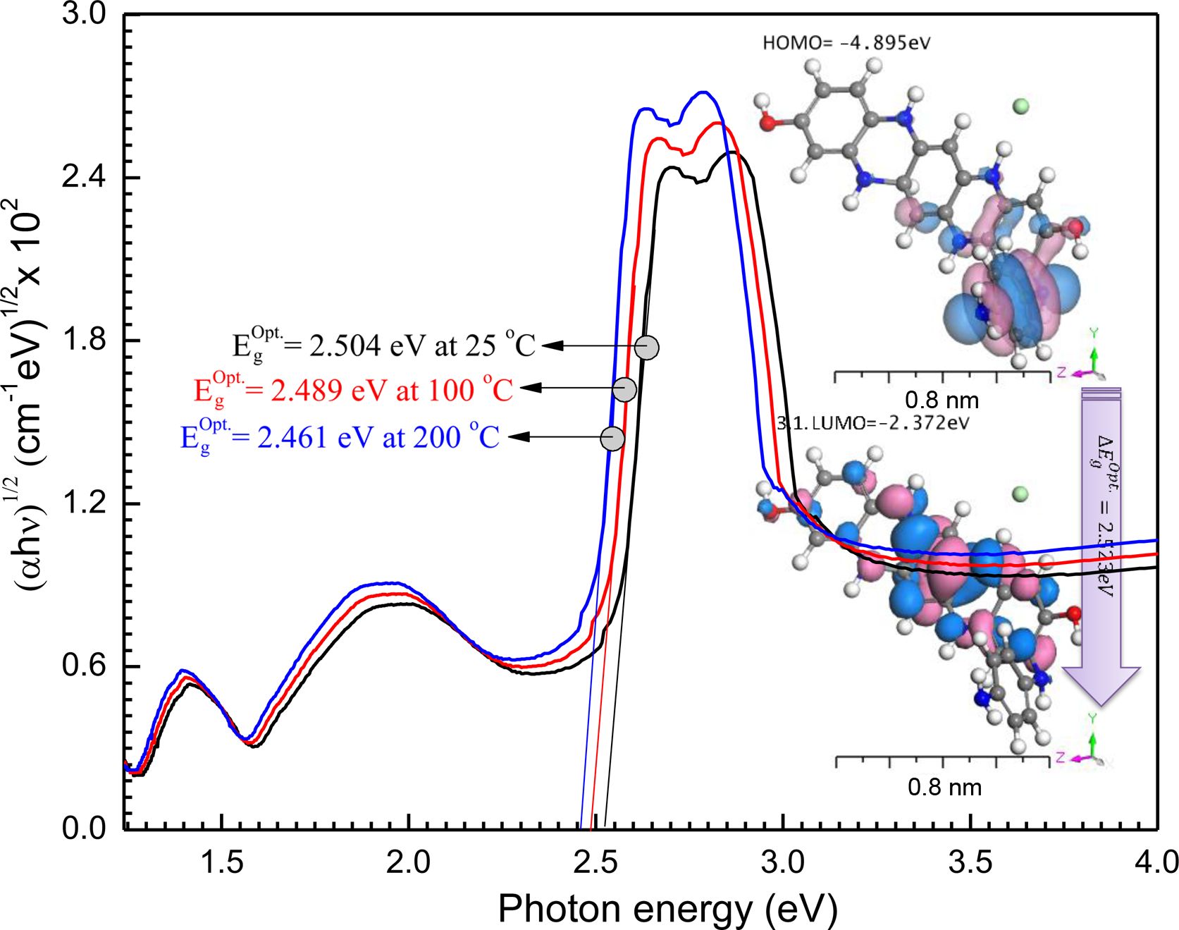
Optical Constants and Dispersion Characterizations: Equation by Bardeen et al. determines the transition types and optical energy gap as ahv = a0(hv- )t; where, α is the absorptivity, hv is the photon energy,
  is the optical energy gap. The direct bandgaps of the [P4A2AP]TF can be expected by plotting the (ahv)1/2 against hv (r = 1/2 allowed direct optical transitions) and extra plotting the linear area of the graph near small energies. When the crystal momentum of electrons and holes in both the conductive and valency bands is the same, the band difference is called “direct”, and an electron will emit a photon directly. The (ahv)1/2 on hν for essential and on set gaps are examined and calculated for various amounts of ½ represented as shown in Figure 6.35 The relationship between (αhν)1/2 vs hν for the film is linear at a strong absorption edge for essential and on set-bands. The straight-line figures of (αhν)1/2 = 0 provide the optical band gap value as represented in Figure 6. As shown in inset Figure 6, the value of
  = 2.523 eV was obtained by DFT calculation using DMol3 program. The computational results and experimental data are in good agreement. Tauc's eq. and the obtained
  can be applied effectively to assess the form of electrical transfer and energy, respectively.36
According to the effect of thermal annealing on the fabricated film, the energy gap values are decreased  = 2.504, 2.489 and 2.461 eV with increasing the annealing temperatures 25, 100, and 200 oC, respectively. We also conclude that, the thermal stability behaviour of the fabricated [P4A2AP]TF increased with increasing the annealing temperatures.
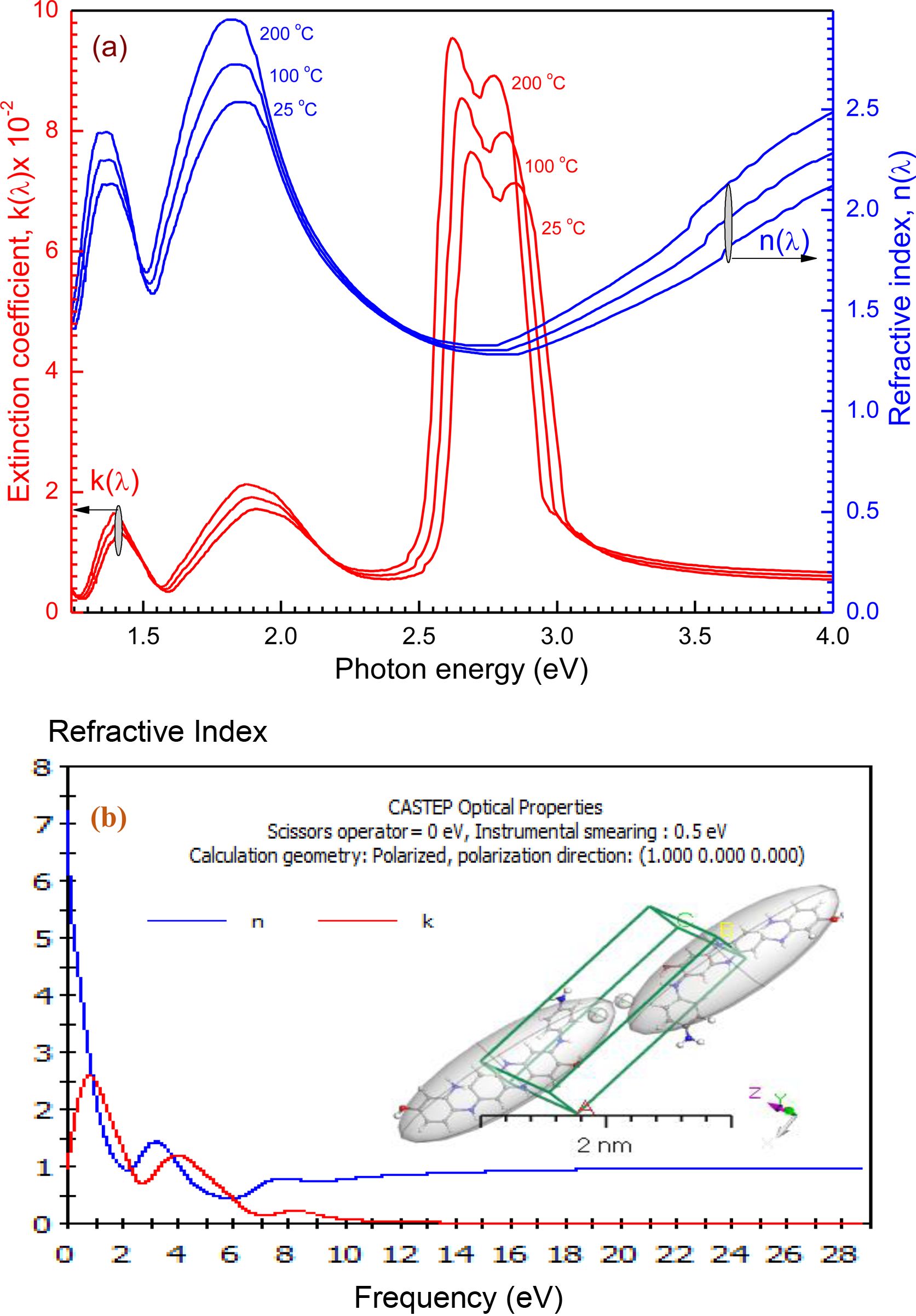
The spectral distribution of the absorption index k(λ) and refractive index n(λ) are represented in Figure 7. The computations of n(λ) and k(λ) were specified for films of thickness nearly from 100 nm. It shows an anomalous dispersion within the range of 300-1000 nm (i.e., corresponding to hv ranged from 1.24 eV to 4.00 eV) exhibiting six absorption peaks at 300 nm < λ < 1000 nm, while, in the UV-visible regions it displays a normal behaviour (multi-oscillator model). The spectral activity of n(λ) translates to natural dispersion at a wavelength of less than 500 nm, since the refractive index decreases rapidly and then starts to rise again. (i.e., the rate of increase becomes nearly strong). In the standard dispersion area, the single oscillator model is applied, and data is utilized to acquire dielectric feature and oscillator factors of high frequency. While, in the UV-visible region the main absorption peak has been obtaining. These are ascribed to electronic transition across π-π* orbitals. For P4A2AP isolated molecule (Figure 7(b)), the DFT was used to assess the values of n(λ) and k(λ), simulated values are quite close to the CASTEP model values achieved through DFT compared to experimental values.
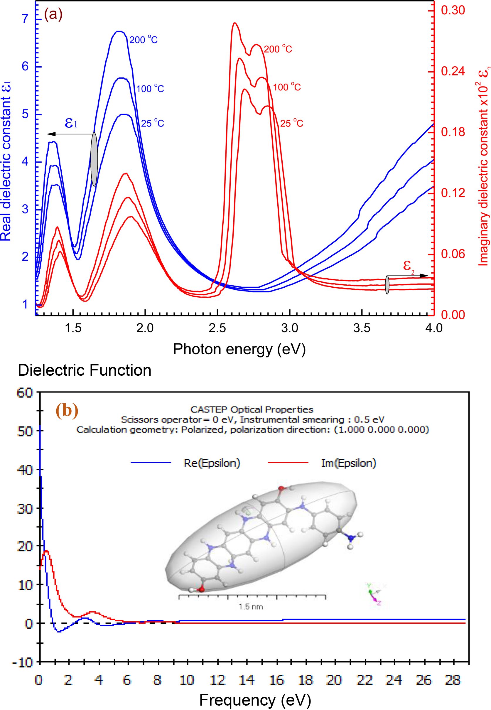
Dielectric Characterization and Optical Conductivity of [P4A2AP]TF Thin Films: The dielectric constant optical parameter ε̅ as the resonant modes or band configuration of any substance gives a dielectric constant spectral difference. The value of ε̅ is related to the nature of optoelectronic instruments.37 The complex of dielectric constant is characterized by the eq.: ε̅ = ereal - ieimj; where, ereal is real dielectric constant, eimj is imaginary dielectric conductivity. ereal (or e1) and eimj. (or e2) components of the dielectric constant are linked to n(λ) and k(λ) by the formula: ereal = n(λ)2-k(λ)2 and eimj = 2n(λ).k(λ). The real component of the dielectric constant is connected to the attenuation of light speed in the material, while in this imaginary component the energy is consumed by an electrical energy field.38 Differences of the real and imaginary components of the complex of dielectric constant ereal, eimj with hv for [P4A2AP]TF are represented in Figure 8. It observed that throughout the whole spectrum of photon energy ranged from 1.25 V to 4.13 eV, ereal > eimj. Unsimilar patterns of the two components of the dielectric constants, particularly in hv range from 2.50 to 6.0 eV, since both ereal and eimj have different behaviours, that illustrates the association between electrons and photons from the light that shows a substantial rise in both curves as a result of the increasing polarization of the thin film at high or low energy wavelengths. Moreover, the diagram is identical to that for the refractive-index graph to the actual dielectric component vs. energy. Based on these interactions, the shapes of ereal and eimj, lead to the creation of peaks or downs in the dielectric spectra that based on the kind of material structure. In the real dielectric component, a maximum peak is observed at 1875 eV. The anomalous dispersal of the refractive index contributes to this. The imaginary dielectric component is shown to increase intensively to 2725 eV. Both ε1(λ) and ε2(λ) calculations using CASTEP technique have a maximum value of @ 60 at a different frequency (eV) @ 6 as demonstrated in Figure 8(b). The results of the experimental and simulation dimensions for the average ε1(λ) and ε2(λ) values are found to be in the frequency range of 1.25-4.13 eV. The DFT was used to assess the values of ε1(λ) and ε2(λ), the simulated values which calculated by the CASTEP model are in good accordance with the experimental parts for the film.
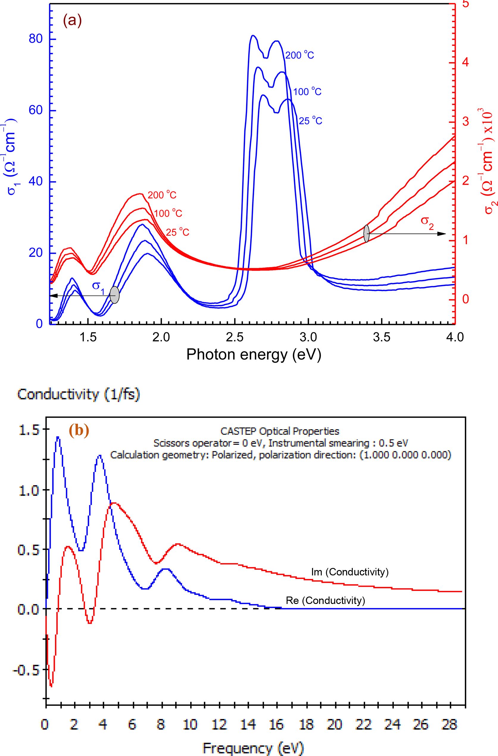
Real conductivity (σ1) and imaginary conductivity (σ2) components of the dielectric constant may be used to measure real and imaginary optical behaviour. They are correlated to the complex dielectric constant and can be given by eq.39: σ*= σ1+iσ2; σ1 = ωε0εimj and σ2 = ωε0εreal; where σ* is the complex optical conductivity, ω is the angular frequency, and εo is the permittivity of free space. εreal and εimj in hv range 1.24 to 4.13 eV as revealed in Figure 9(a), 9(b). From Figure 9(a), the pattern can be divided into two sections: section(I) ranged from n 1.25 to 2.40 eV both σ1 and σ2 have the same behaviour characterized by six peaks. Section (II) after hv > 2.50 eV the spectra demonstrate an opposite tendency of the two components of optical conductivity, since s1 has its maximum broadband in hv range from 2.40 to 3.10 eV. After, hv > 3.1 eV, σ1 begins to increase slightly with the increase of hv. On the other hand, after hv > 3.1 eV, σ2 rapidly increases with the increase of hv up to 4.5 eV it starts to increase slightly. The imaginary-component of (σ*) has a larger value that corresponds to the real component of the dielectric constant. After hv = 3.25 eV, with enhancing hv, a frequent increase of σ*. This ascending is because of the electrons excited by hv. The source of an increase due to some differences in the film structure caused by the charging effect.
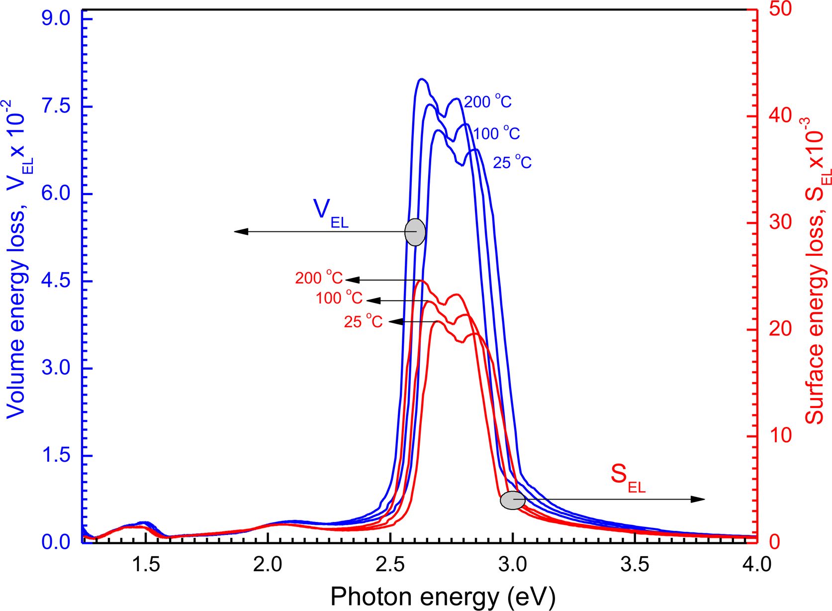
Surface energy loss function (SELF) and volume energy loss function (VELF) are significant considerations when analyzing the rate of energy loss in high-energy electrons that pass through a substance and record the following equations:40,41 VELF =  and SELF =
  . The hv depends on the surface energy and volume loss functions for the film with 100 nm shown in Figure 10. The figure indicates the energy loss by the free charge carriers when transferring the surface particularly for relatively smaller energies with the same efficiency through the bulk material.42 Furthermore, there is no important variation among SELF and VELF at lower and higher hv but the SELF decreases more than at the VELF specific peaks.
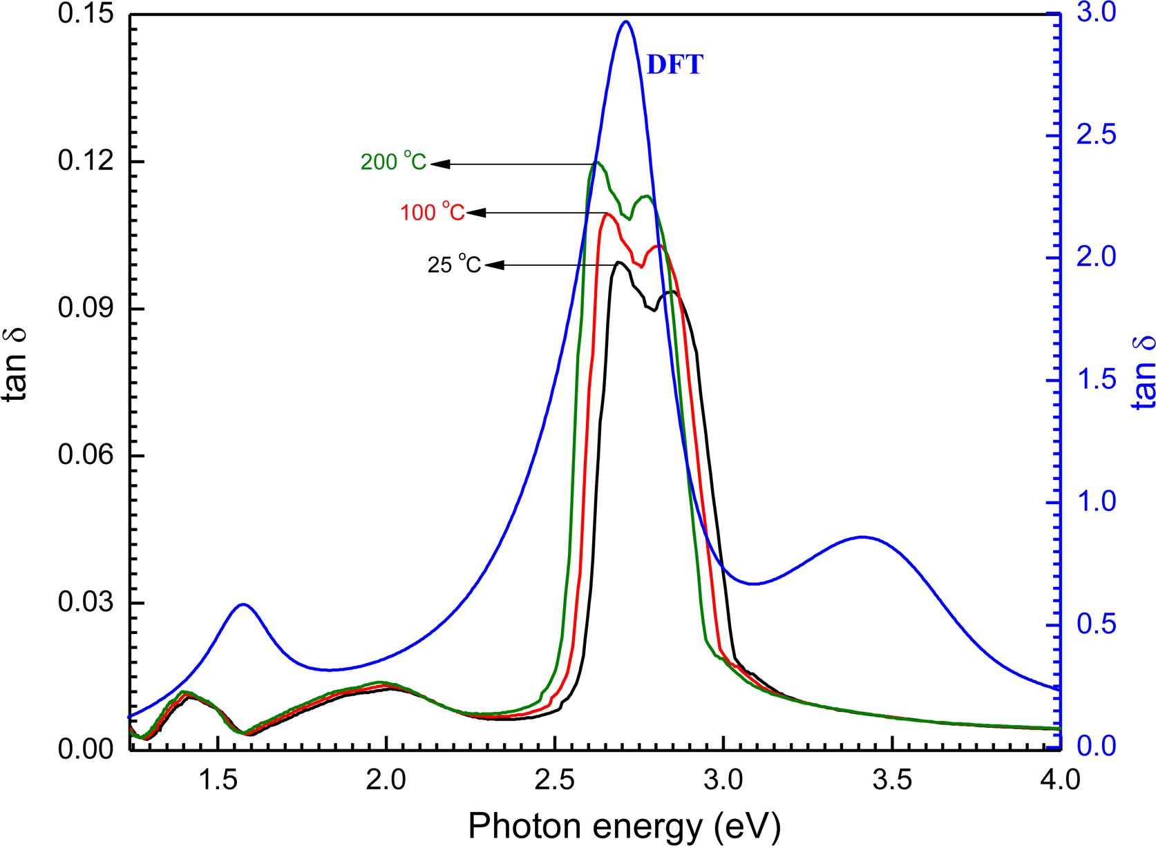
The loss factor (tan δ) of film has been calculated using this equation: tan δ = ε2/ε1 from the values of ε1 and ε2. Since loss coefficient is directly proportional with ε2 and inversely proportional with ε1. From the figure it is clear that tan d is approximately has the same trend as ε2. The effect of the real dielectric constant on tan d could be negatable. The difference in the loss factor tan d with photon energy (ranged from 1.25 to 4.13 V) for the samples of [P4A2AP]TF is shown in Figure 11. The loss coefficient is defined by an essential sharp peak in hv ranged from 2.50 to 3.25 eV. The simulated values obtained by CASTEP/DFT which calculated tan d are in good accordance with the experimental amounts for the [P4A2AP]TF (Figure 11).
Finally, the dependency of the complex dielectric constant, optical conductivity, and loss factor parameters for the [P4A2AP]TF after annealing at 100 and 200 oC for 1 h has been studied. It is observed that the values of the optical parameters are increasing with increasing the annealing temperature on the fabricated film. This rise in optical parameters can be caused by electrons stimulated by photon energy incident. Any changes to the film structure caused by the charge order effect may be the cause of the rise.
|
Figure 1 Combined experimental FTIR [P4A2AP]TF spectra and simulated IR by utilizing Gaussian 09W with DFT/WB97XD and basis set 6-311G |
|
Figure 2 TGA and DrTGA thermogram of the doped P4A2AP |
|
Figure 3 (a) SEM image for [P4A2AP]TF at 100 nm at 25 oC; (b) at 100 oC; (c) at 200 oC; (d) side view of the same selected image with the thickness ≡ 100 nm. |
|
Figure 4 Experimental UV/Vis spectrum for [P4A2AP]TF thin-film
of thickness 100 nm at different thermal annealing; inset figure simulated UV/Vis spectrum for P4A2AP isolated molecule using
DMOl3
/DFT. |
|
Figure 5 The relation T(λ) and R(λ) vs wavelength of the fabricated film at different thermal annealing temperature. |
|
Figure 6 Relation between (αhv) 0.5 and hv for [P4A2AP]TF at different thermal annealing, inset figure is the theoretical calculation HOMO and LUMO for (P4A2AP) isolated molecule in a gaseous phase. |
|
Figure 7 (a) The dispersion curve of n(λ) and k(λ) for the thin film at different thermal annealing temperature; (b) The simulated n and k vs hν eV of isolated molecule copolymer by CASTEP/DFT. |
|
Figure 8 (a) The ε1 and ε2 vs hv of [P4A2AP]TF of 100 nm thickness at different thermal annealing temperature; (b) Simulation dielectric function for P4A2AP by utilizing CASTEP technique. |
|
Figure 9 (a) hv dependence of both and of the film of thickness 100 nm at different thermal annealing temperature; (b) Simulation optical conductivity function for the film by utilizing CASTEP technique. |
|
Figure 10 SELF and VELF functions on hv for the film at different thermal annealing temperature. |
|
Figure 11 Loss factor (tan δ) with photon energy (hv) for [P4A2AP]TF at different thermal annealing temperature. Inset figure is the theoretical calculation loss function for P4A2AP isolated molecule in gaseous phase by using CASTEP/ DFT computations. |
Poly(p-phenylenediamine-co-o-aminophenol) has been synthesized by chemical methods using oxidative polymerization method in high acidic medium using ferric chloride as an oxidizing agent. Thin-film with ≡ 100 ± 2 nm of the considered copolymer has been fabricated by spin coating method. Thin-film was annealed at different temperatures. Different characterization techniques for the thin film-like FTIR, UV-Vis spectroscopy and optical properties have been studied in detail. The resulted XRD data have been employed to study the interface. DFT was used for optimization by DMol3 and CASTEP. Spectroscopic and structural characteristics for the thin film have confirmed the chemical composition and XRD observations revealed the same crystal structure. Combined between experimental and TDD-DFT data, the average crystallite size and composite interface are 71.87 nm and orthorhombic symmetry (a=7.38(2); b=18.09(6); c=26.09(4) Å and α=β=γ=90o) with space group (Pmcn) for the thin film. The calculated by DFT and experimental were found to be 2.523 and 2.504 eV for as-isolated crystals and the thin film of the copolymer, respectively. The electronic transition of the thin film was found a direct allowed transition. The optoelectrical parameters have been calculated for the film including refractive index, extinction coefficient, dielectric constant, and optical conductivity. Increasing the annealing temperature, the optical band gap values are decreased, that may be leads to an enhancement thermal stability of the lattice parameter. CASTEP simulated values are consistent with the experimental values for optical parameters of the thin film. Based on these results, the fabricated thin film can be used as a candidate material for optoelectronic devices and solar cells.
- 1. Sherman, B. C.; Euler, W. B.; Force, R. R. The Modern Student Laboratory: Polyaniline-A Conducting Polymer: Electrochemical Synthesis and Electrochromic Properties. J. Chem. Ed. 1994, 71, A94.
-

- 2. Nalwa, H. S. Handbook of Advanced Electronic and Photonic Materials and Devices, Ten-Volume Set, Academic Press 2000.
-
- 3. Panah, N. B.; Mahjani, M. G.; Jafarian, M. Correlation between Irregular Surface Geometry and Certain Electrochemical Quantities in Poly-ortho-aminophenol. Prog. Org. Coat. 2009, 64, 33-38.
-
- 4. Wang, C. Y.; Mottaghitalab, V.; Too, C. O.; Spinks, G. M.; Wallace, G. G. Polyaniline and Polyaniline-Carbon Nanotube Composite Fibres as Battery Materials in Ionic Liquid Electrolyte. J. Power Sources 2007, 163, 1105-1109.
-
- 5. Hu, H.; Ortíz-Aguilar, B. E.; Hechavarría, L. Effect of pH Value of Poly(ethylenimine)-H2SO4 Electrolyte on Electrochromic Response of Polyaniline Thin Films. Opt. Mater. 2007, 29, 579-584.
-
- 6. Huang, H.; Zheng, Z.; Luo, J.; Zhang, H.; Wu, L.; Lin, Z. Internal Photoemission in Polyaniline Revealed by Photoelectrochemistry. Synth. Met. 2001, 123, 321-325.
-
- 7. Forrest, S. R. Active Optoelectronics Using Thin-film Organic Semiconductors. IEEE J. Sel. Top. Quantum Electron. 2000, 6, 1072-1083.
-
- 8. Iqbal, N.; Sagar, S.; Khan, M. B.; Bassyouni, M. I.; Khan, Z. M. Aluminum Silicate Fibers Impregnated Acrylonitrile Butadiene Rubber Composites: Ablation, Thermal Transport/Stability, and Mechanical Inspection. J. Appl. Polym. Sci. 2013, 130, 4392-4400.
-
- 9. Singh, N.; Singh, S.; Ashraf, S.; Riaz, U. Experimental and Theoretical Studies of Benzoquinone Modified Poly(ortho-phenylenediamine): Singlet Oxygen Generating Oligomers. Colloid Polym. Sci. 2020, 298, 1443-1453.
-
- 10. El Azab, I.; Thabet, H. K.; Almotairi, S. A.; Saleh, M.; Mogharbel, R.; Mahmoud, S.; El-Rayyes, A.; Ibrahim, A.; Zoromba, M. S.; Abdel-Aziz, M. H.; Ibrahim, S. M.; Al-Hossainy, A. F. Synthesis of a novel coumarin heterocyclic derivative and fabrication of hybrid nanocomposite thin film with CoOFe2O4 for optoelectronic applications. J. Mol. Struct. 2021, 1241, 130640.
-
- 11. Mu, S.; Zhang, Y.; Zhai, J. The Electrochemical Copolymerization of Aniline with 2,4-Diaminophenol and the Electric Properties of the Resulting Copolymer. Electrochim. Acta 2009, 54, 3923-3929.
-
- 12. Zoromba, M. Sh.; Abdel-Aziz, M. Ecofriendly Method to Synthesize Poly(ο-aminophenol) Based on Solid State Polymeri- zation and Fabrication of Nanostructured Semiconductor Thin Film. Polymer 2017, 120, 20-29.
-
- 13. Hua, F.; Ruckenstein, E. Highly Soluble Conducting Poly(Ethylene oxide) Grafted at Two Sites of Poly(o-aminobenzyl alcohol). J. Polym. Sci. Part A 2004, 42, 4756-4764.
-
- 14. Zoromba, M. Sh. Novel and Economic Acid-Base Indicator based on (p-toluidine) oligomer: Synthesis; Characterization; photoluminescence and Solvatochromism Applications. Spectrochim. Acta A Mol. Biomol. Spectrosc. 2017, 187, 61-67.
-
- 15. Zhang, J.; Shan, D.; Mu, S. Chemical Synthesis and Electric Properties of the Conducting Copolymer of Aniline and o-Aminophenol. J. Polym. Sci. Part A Polym. Chem. 2007, 45, 5573-5582.
-
- 16. Zoromba, M. Sh.; Alghool, S.; Abdel‐Hamid, S. M. S.; Bassyouni, M.; Abdel‐Aziz, M. H. Polym. Adv. Technol. 2017, 28, 842-848.
-
- 17. Zoromba, M. Sh.; El-Ghamaz, N. A. Samir Alghool. J. Inorg. Organomet. Polym. Mater. 2015, 25, 955-963.
-
- 18. Liu, J.; Guo, T.-F.; Yang, Y. Effects of Thermal Annealing on the Performance of Polymer Light Emitting Diodes. J. Appl. Phys. 2002, 91, 1595-1600.
-
- 19. Al-Hossainy, A. F.; Ibrahim, A. The Effects of Annealing Temperature on the Structural Properties and Optical Constants of a Novel DPEA-MR-Zn Organic Crystalline Semiconductor Nanostructure Thin Films. Opt. Mater. 2017, 73, 138-153.
-
- 20. Zhang, G.; Lu, K.; Zhang, X.; Yuan, W.; Shi, M.; Ning, H.; Tao, R.; Liu, X.; Yao, R.; Peng, J. Effects of Annealing Temperature on Optical Band Gap of Sol-gel Tungsten Trioxide Films. Micromachines 2018, 9, 377.
-
- 21. Titov, A. A.; Filippov, O. A.; Smol'yakov, A. F.; Averin, A. A.; Shubina, E. S. Synthesis, Structures and Luminescence of Multinuclear Silver (i) Pyrazolate Adducts with 1,10-Phenanthroline Derivatives. Dalton Trans. 2019, 48, 8410-8417.
-
- 22. Sebastian, S.; Sundaraganesan, N. The Spectroscopic (FT-IR, FT-IR Gas Phase, FT-Raman and UV) and NBO Analysis of 4-Hydroxypiperidine by Density Functional Method. Spectrochim. Acta A Mol. Biomol. Spectrosc. 2010, 75, 941-952.
-
- 23. Zoromba, M. S.; Tashkandi, M.; Alshehri, A.; Abdel-Aziz, M.; Bassyouni, M.; Mahmoud, S.; Slimane, A. B.; Al-Hossainy, A. Polymer Solar Cell Based on Doped o-anthranilic Acid and o-aminophenol Copolymer. Opt. Mater. 2020, 104, 109947.
-
- 24. Gospodinova, N.; Terlemezyan, L. Conducting Polymers Prepared by Oxidative Polymerization: Polyaniline. Prog. Polym. Sci. 1998, 23, 1443-1484.
-
- 25. Le Bihan, M. T. Contribution a l'étude Structurale des Sulfures d'arsenic et de Plomb. Structure de la Baumhauerite. Acta Crystallogr. 1961, 14, 1210-1211.
-
- 26. Stark, W.; Jaunich, M. Investigation of Ethylene/Vinyl Acetate Copolymer (EVA) by thermal analysis DSC and DMA. Polym. Test. 2011, 30, 236-242.
-
- 27. Kim, S. H.; Park, Y. C.; Jung, G. H.; Cho, C. G. Characterization of Poly(styrene-b-vinylbenzylphosphonic acid) Copolymer by Titration and Thermal Analysis. Macromol. Res. 2007, 15, 587-594.
-
- 28. Al-Hossainy, A. F.; Ibrahim, A. The Effects of Annealing Temperature on the Structural Properties and Optical Constants of a Novel DPEA-MR-Zn Organic Crystalline Semiconductor Nanostructure Thin Films. Opt. Mater. 2017, 73, 138-153.
-
- 29. Makhlouf, M.; El-Denglawey, A.; Zeyada, H.; El-Nahass, M. The Structural and Optical Characterizations of Tetraphenylporphyrin Thin Films. J. Lumin. 2014, 147, 202-208.
-
- 30. Kasha, M.; Rawls, H.; El-Bayoumi, M. A. The Exciton Model in Molecular Spectroscopy. Pure Appl. Chem. 1965, 11, 371-392.
-
- 31. Pietrangeli, D.; Rosa, A.; Ristori, S.; Salvati, A.; Altieri, S.; Ricciardi, G. Carboranyl-porphyrazines and Derivatives for Boron Neutron Capture Therapy: From Synthesis to in vitro Tests. Coord. Chem. Rev. 2013, 257, 2213-2231.
-
- 32. Scheidt, W. R. Explorations in Metalloporphyrin Stereochemistry, Physical Properties and Beyond. J. Porphyr. Phthalocyanines 2008, 12, 979-992.
-
- 33. Bourezgui, A.; Al-Hossainy, A.; Azab, I. El; Alresheedi, F.; Mahmoud, S.; Bassyouni, M.; Abdel-Aziz, M.; Zoromba, M. Sh. Combined Experimental and TDDFT Computations for the Structural and Optical Properties for Poly(ortho phenylene diamine) Thin Film with Different Surfactants. J. Mater. Sci. Mater. Electron. 2021, 32, 5489-5503.
-
- 34. Zoromba, M. Sh.; Alshehri, A.; Al-Hossainy, A.; Abdel-Aziz, M. Doped-poly(anthranilic acid-co-o-phenylene diamine) Thin Film for Optoelectronic Applications. Opt. Mater. 2021, 111, 110621.
-
- 35. Aflaki, M.; Davar, F. Synthesis, Luminescence and Photocatalyst Properties of Zirconia Nanosheets by Modified Pechini Method. J. Mol. Liq. 2016, 221, 1071-1079.
-
- 36. Zoromba, M. Sh.; Al-Hossainy, A.; Abdel-Aziz, M. Conductive Thin Films Based on Poly(aniline-co-o-anthranilic acid)/Magnetite Nanocomposite for Photovoltaic Applications. Synth. Met. 2017, 231, 34-43.
-
- 37. Zhokhavets, U.; Goldhahn, R.; Gobsch, G.; Schliefke, W. Dielectric Function and One-dimensional Description of the Absorption of Poly(3-octylthiophene). Synth. Met. 2003, 138, 491-495.
-
- 38. Al-Hossainy, A.; Zoromba, M. Sh.; Abdel-Aziz, M.; Bassyouni, M.; Attar, A.; Zwawi, M.; Abd-Elmageed, A.; Maddah, H.; Slimane, A. B. Fabrication of Heterojunction Diode Using Doped-poly(ortho-aminophenol) for Solar Cells Applications. Physica B Condens. Matter 2019, 566, 6-16.
-
- 39. Caglar, Y.; Ilican, S.; Caglar, M. Single-oscillator Model and Determination of Optical Constants of Spray Pyrolyzed Amorphous SnO2 Thin Films. Eur. Phys. J. B 2007, 58, 251-256.
-
- 40. Al-Hossainy, A.; Bassyouni, M.; Zoromba, M. S. Elucidation of Electrical and Optical Parameters of Poly(o-anthranilic acid)-poly (o-amino phenol)/Copper Oxide Nanocomposites Thin Films. J. Inorg. Organomet. Polym. Mater. 2018, 28, 2572-2583.
-
- 41. Al-Hossainy, A.; Zoromba, M. S.; El-Gammal, O.; El-Dossoki, F. I. Density Functional Theory for Investigation of Optical and Spectroscopic Properties of Zinc-quinonoid Complexes as Semiconductor Materials. Struct. Chem. 2019, 30, 1365-1380.
-
- 42. El-Nahass, M.; Ammar, A.; Atta, A.; Farag, A.; El-Zaidia, E. Influence of X-ray Irradiation on the Optical Properties of CoMTPP Thin Films. Opt. Commun. 2011, 284, 2259-2263.
-
- Polymer(Korea) 폴리머
- Frequency : Bimonthly(odd)
ISSN 0379-153X(Print)
ISSN 2234-8077(Online)
Abbr. Polym. Korea - 2023 Impact Factor : 0.4
- Indexed in SCIE
 This Article
-
2021; 45(4): 541-551
Published online Jul 25, 2021
- 10.7317/pk.2021.45.4.541
- Received on Feb 11, 2021
- Revised on Mar 14, 2021
- Accepted on Apr 4, 2021
Services
- Full Text PDF
- Abstract
- ToC
- Acknowledgements
- Supporting Information
Introduction
Experimental
Results and Discussion
Conclusion
- References
Shared
Correspondence to
- Al-Hossainy
-
Department of Chemistry, Faculty of Science, Northern Border University, 13211 Arar, Saudi Arabia
- E-mail: ahmed73chem@scinv.au.edu.eg
- ORCID:
0000-0001-5531-6940
Hyecheon Building(Room 601), #354, Gangnam-Daero, Gangnam-Gu, Seoul 06242, Korea
TEL : 82-2-568-3860, 561-5203, 569-3860 FAX : 82-2553-6938 E-mail: polymer@polymer.or.kr